I am trying to learn more about logical state initialization, logical operators, and measurement for the surface code. I am having some trouble understanding the nitty-gritty details of the logical $\pm Y_L$ initialization and logical $Y$ measurement.
I started my investigation from here : How are logical operators performed and measured on the surface code, in a defect-free way?
Which I found to be pretty clear with respect to the $\pm Z_L$ and $\pm X_L$ initialization and measurements.
For the $Y$ logical initialization and measurement, the answer refers to the paper Inplace Access to the Surface Code Y Basis, which I found to be somewhat confusing. I believe this is due to my lack of understanding with regards to the "defect diagrams" in the paper.
I was able to find this helpful slide-deck on Understanding Defect Diagrams, from this post What is the point of defect diagrams?.
Now, for the $Y_L$ basis initialization and measurement, I am looking at the "Y Basis Memory Experiment" portion of this figure from the aforementioned paper:
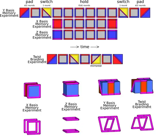
I think that the first three "slices" of the $Y$ memory circuit are the $Y_L$ initialization; however, I would like some clarification on how these slices are implemented and how you obtain $+Y_L$ or $-Y_L$ specifically.
- In the first slice, my understanding is that the data qubits in the red region will be reset to $+X$ and the data qubits in the blue region will be reset to $+Z$; now, are the qubits along the pink diagonal reset to $+Y$? do you reset them to $+Y$ if you want to initialize $+Y_L$ and reset them to $-Y$ if you want to initialize $-Y_L$? If you do not reset the data qubits along the diagonal to $\pm Y$, what do you set them to?
- Now, for the second slice, my understanding is that you will "turn on"/measure the stabilizers depicted in the bottom-right figure of this diagram for $d/2$ rounds, using the standard surface code stabilizer measurement circuit and schedule.
- For the third slice, labeled switch, I understand that this step is related to the circuit steps shown in the preceding figure; however, it is not clear to me how you go in reverse, if that is even the right way of thinking about it.
The $Y$ basis measurement would then seem to be composed of the last three slices of the $Y$ Memory sequence.
- The step labeled switch, would seem to be the circuit steps shown in the preceding figure, directly as shown.
- The next step would then seem to be $d/2$ rounds of standard surface code stabilizer measurement for the stabilizers shown in the bottom-right figure of the preceding diagram. Essentially the same as the second step in the initialization.
- Finally, it would seem you measure the data qubits in the red region in the $X$ basis, and data qubits in the blue region in the $Z$ basis. So, then, do you measure the data qubits along the diagonal in the $Y$ basis? Is the logical $Y$ measurement outcome then the product of these single qubit $Y$ basis measurements along the diagonal?
Logical Phase (S) gate clarification:
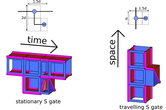
Firstly, I am unclear on how the second "traveling S gate" would work in practice; I just don't understand the defect diagram.
Secondly, for the stationary S gate, I would like some clarification on the steps:
- First, you extend the logical patch down, so you have a d x 2d patch, perform d rounds of standard surface code stabilizer measurements.
- Next, it seems that the two patches are split, followed by a $Y$ basis measurement on the lower patch.
- Question, is there any conditional operation on the un-measured logical patch, depending on the $Y$ basis measurement outcome?
Thank you for taking the time to look over this and I appreciate all of your time and assistance.
