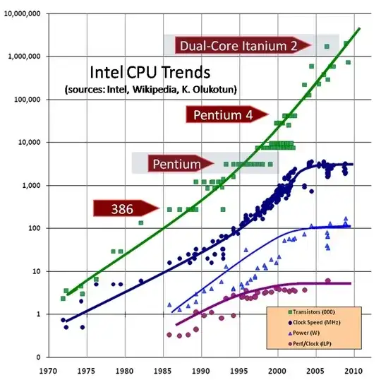
There are two different "laws" being graphed here, Moore's law, and Dennard scaling. Moore's law is an economic observation, made by Gordon Moore in 1965, that predicts that the number of transistors on a die will tend to double about every two years. It does not seem to be slowing down (yet). While there are reasons to believe that transistors will stop scaling down soon (14nm is 140 Angstroms (about the width of 140 hydrogen atoms)) it may be possible to continue Moore's law scaling for some time, either by making bigger chips (what Moore originally predicted) or by stacking multiple layers of transistors in the 3rd dimension.
Dennard Scaling, on the other hand, is an observation, made by Robert Dennard in 1974 that every time you scale down the width of a CMOS gate by a factor of 2, you can reduce both supply voltage and the threshold voltage by a factor of 2, the clock frequency can improve by a factor of 2, and the power density will stay constant. (Or you can scale down the voltage by less than 2, and you'll get a better than 2x clock frequency boost, but an increase in power.) When Dennard's observation was made a CMOS transistor was about 5 micron = 5000 nm wide. (So we've scaled transistor widths by a factor of about 360 in about 40 years.)
The limit that showed up in the early 2000s has to do with threshold voltage. Clock frequency (at a particular transistor size) is at best proportional to
$V_{dd} - V_{th}$ (supply voltage minus threshold voltage), but as you scale $V_{th}$ down leakage current (and power) increases exponentially. That was fine from 1974 to about 2000 because $V_{dd}$ was much larger than $V_{th}$. (In 1974 $V_{dd}$ was usually about 12V.) So we could hold $V_{th}$ at around a volt or so, and just change $V_{dd}$. But now with $V_{dd}$ around 1.3V and $V_{th}$ around .5V, we can't scale voltage much anymore (without dramatically increasing leakage power.)